
Wide-bandgap device research and development at SRL
Our research group is currently working on the following III-Nitride (III-N) projects:
- III-N vertical electronic switches for kV-range power applications
- III-N bipolar transistor technology
- III-N UV avalanche photodetectors in linear-mode and Geiger-mode operations
- UV lasers
What are wide-bandgap semiconductors?
Wide-bandgap semiconductors in general refer to any semiconductor materials with an energy bandgap much greater than conventional semiconductors such as silicon (Si) and gallium arsenide (GaAs). These wide-bandgap materials are typically compound semiconductors such as gallium nitride (GaN), aluminum gallium nitride (AlGaN), indium gallium nitride (InGaN), or silicon carbide (SiC). A notable wide-bandgap material that is not a compound semiconductor is carbon (C) in one of its covalent bonded forms, diamond. These materials usually have a bandgap greater than 3 electron volts (eV), compared with 1.12 eV for silicon and 1.43 eV for GaAs.
Why wide-bandgap devices?
Wide-bandgap semiconductor technologies have actively been sought as the next generation semiconductors due to their inherent wide bandgap, high electron saturation velocity, high thermal conductivity, and wide temperature operation range capabilities. For example, a wide bandgap semiconductor can sustain high temperature operation up to about 300 C. Compare this with a maximum temperature of roughly 100 C for silicon-based microelectronics. This property will enable microelectronic systems to more easily operate in elevated ambient temperature environments such as power plants and hybrid electric vehicles (HEVs). Additionally, the critical electric field for wide-bandgap materials is typically ten times higher than that for any current commercially available semiconductor technology. This feature will allow wide-bandgap electronic circuits to operate at very high voltages with high power amplification efficiency. Recently, the GaN-based heterojunction field effect transistor (HFET) has been developed for next-generation base transmission stations for wireless communication standards such as GSM, EDGE, and W-CDMA.
In optoelectronic applications, wide-bandgap materials have been the only viable choices for efficient green and blue light emitting diodes (LEDs) and lasers. The green and blue LED provide the “missing” colors for the traditional LED (which can only offer colors between yellow and red) and offer immense opportunities for future energy-efficient solid-state lighting. Blue laser diodes will be the work horse of the next-generation high-density DVD reader heads as well. In the shorter wavelength regime, wide-bandgap semiconductor-based solid-state light sources and detectors provide many important applications such as UV-light germicide sources for water sanitation applications and advanced solar-blind optical communication systems.
What we do
The wide-bandgap materials are, however, relatively immature compared to current commercialized semiconductor technologies such as silicon, gallium arsenide (GaAs), and even indium phosphide (InP). Due to the tremendous commercialization opportunities for wide bandgap semiconductors in next-generation microelectronics and optoelectronics, they are currently under substantial research and development efforts.
The major technology development hurdles for wide-bandgap material systems have been concentrated in two major areas: material technology and robust device design and fabrication technology. The research done here at SRL group will focus on the development of a variety of GaN-based semiconductor device fabrication technologies and close collaboration with strong material epitaxial research groups at Georgia Tech to form a vertically integrated semiconductor development infrastructure.
Currently the SRL group is developing GaN-base HBT technology for both RF power applications and high-voltage electronics for harsh environments. In optoelectronic technology development, a GaN-based single photon (Geiger mode) deep UV detector will be investigated.
Nanoscale semiconductor devices—high-speed or high-power
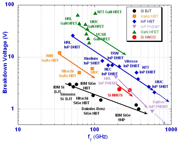
fT vs breakdown voltage plot for current viable semiconductor transistor technologies (M. Feng, S. Shen, D. Caruth, and J. Huang, Proc. IEEE, Feb., 2004)
Modern microelectronics developments have been highly concentrated in two regimes: high-power and high-speed operation. This rationale can be explained in the chart. For a given device technology, an increase in the device operating speed can be engineered through drastic device scaling at the cost of maximum operating voltage. Advanced silicon technology, for example, is capable of operation over 350 GHz using the SiGe alloy. However, the device breakdown voltage is reduced to below 2 volts accordingly. The breakdown voltage limits the maximum available power amplification at high frequency and also sets a speed ceiling for digital circuits at around 200 GHz. GaN and related materials, on the other hand, have a very high critical electric field when compared with currently available semiconductor material systems like silicon, GaAs, and InP. GaN-based devices promise high power amplification in lower frequency bands and high-speed digital and analog applications at terahertz-range frequencies in the future.

picture of a 0.12 µm T-gate on GaAs MESFET using direct E-beam photolithography.
The prior work of Dr. Shen on the ion-implanted GaAs MESFET demonstrated a fT > 142 GHz and fMAX > 235 GHz with a gate length of 0.12 micron. He has also developed a proprietary commercial-grade InP HBT-based 40 Gb/s optoelectronic integrated circuit (OEIC) fabrication technology in the past few years. These achievements and experiences were leveraged to further the development of new III-N devices and integrated circuits in the SRL. With intensive collaboration with the world-class material growth groups at Georgia Tech, we also plan to leverage our past research experience and the advanced e-beam equipment at IEN at Georgia Tech to forge ultra high-speed GaN-based nanoscale transistors. The ultimate goal is to implement GaN-related semiconductor devices for next-generation III-N mm-wave and high-energy-efficient integrated circuits.
We are currently pushing the GaN-based technology envelope into the high voltage and high power regimes for future energy-efficient power electronics. Recently, by collaborating with Prof. Russell Dupuis at Georgia Tech, his group also demonstrated the first InGaN-based HBTs with a cutoff frequency (fT) of greater than 5.3 GHz and a maximum power density of greater than 3 MW/cm2 was also achieved in his group. (110322)